
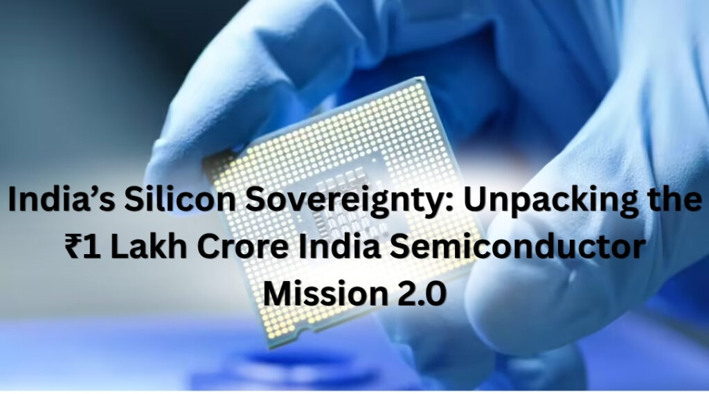
India gives ₹1 lakh crore to Semiconductor Mission 2.0 to build a strong chip ecosystem and cut down on imports.
- Blog Industry New Launch Trending News
- Entrepreneurs Story
- April 4, 2026
- 37
- 13 minutes read
Semiconductors have emerged as the defining resource of the modern technology era, powering everything from the smartphones in our pockets to the advanced defence systems that protect our national borders. Recognising this strategic reality, the Government of India has significantly raised its ambitions. The India Semiconductor Mission 2.0 has received an approved outlay of approximately ₹1.2 lakh crore, signalling a decisive shift: India is no longer content to be a consumer of technology — it is positioning itself as a global leader in the silicon value chain.
This strategic evolution aims to accelerate domestic chip manufacturing, reduce India’s multi-billion dollar semiconductor import bill, and build a resilient, self-sufficient ecosystem capable of withstanding geopolitical disruptions in global supply chains.
The Strategic Evolution: From ISM 1.0 to 2.0
The India Semiconductor Mission (ISM) 1.0, launched in December 2021 with a budget of ₹76,000 crore, laid the essential groundwork. Its primary achievement was establishing India’s credibility as a semiconductor destination, attracting landmark investments from the Tata Group and Micron Technology. ISM 2.0 builds on this foundation with a far more comprehensive, “full-stack” approach.
Where ISM 1.0 was about establishing a presence, ISM 2.0 is about asserting technological leadership. The second phase prioritises the following areas:
- Advanced Node Manufacturing: Providing incentives to progressively advance from the currently approved 28nm–65nm fabrication nodes toward more cutting-edge chip manufacturing capabilities over the long term.
- Research, Development, and IP Creation: Moving beyond contract manufacturing to owning the intellectual property behind chip design.
- Supply Chain Integration: Supporting domestic production of specialised chemicals, gases, and semiconductor manufacturing equipment to reduce import dependency.
Strengthening the Ecosystem of Chip Fabrication Companies in India
Private sector participation is central to the mission’s success. The landscape of chip fabrication companies in India is undergoing a significant transformation, with major domestic and international players collaborating to establish fabrication plants (“Fabs”) that were once considered impractical in India.
The government has allocated an additional ₹8,000 crore under its Modified Programme for Semiconductors and Display Fab Ecosystem for FY 2025–26. This funding helps chip fabrication companies manage the extremely high capital barriers to entry and the prolonged gestation periods inherent to this industry.
It is important to note that while Micron Technology’s facility in Sanand, Gujarat, represents a major milestone, it operates as an Assembly, Testing, Marking and Packaging (ATMP) unit — not a full fabrication plant. It is a critical first step in building India’s semiconductor ecosystem, and further upstream investment in wafer fabrication remains a priority.
Key Pillars of the ISM 2.0 Strategy
- Nurturing the Fabless Ecosystem
The government aims to support up to 100 domestic fabless companies over five years through the Design Linked Incentive (DLI) scheme. This ensures that companies without their own fabrication facilities can still innovate and design chips that are manufactured domestically.
- Modernisation of Infrastructure
A dedicated ₹900 crore has been earmarked to modernise the Semiconductor Laboratory (SCL) in Mohali, transforming it into a world-class centre for research and prototyping.
- Human Capital Development
The mission extends well beyond physical infrastructure. Strategic partnerships with leading universities and engineering institutions are creating a sustained pipeline of VLSI (Very Large Scale Integration) engineers equipped to compete in the global workforce.
Economic Impact and Import Substitution

India’s dependence on semiconductor imports has long been a structural vulnerability in its economy. The government is addressing this by targeting domestic production to meet 70–75% of the country’s semiconductor requirements — across automotive, mobile, and consumer electronics applications — by 2029.
ISM 2.0 is projected to deliver significant economic dividends:
- Job Creation: Thousands of specialised, high-paying engineering and manufacturing positions across the semiconductor value chain.
- Foreign Direct Investment: Substantial FDI from global corporations pursuing supply chain diversification strategies beyond China — a trend widely observed across the technology sector.
- GDP Contribution: India’s broader electronics manufacturing sector is projected to become a $500 billion industry by 2030, with semiconductors as a key enabler of that growth.
Frequently Asked Questions (FAQs)
1. What is the main goal of the India Semiconductor Mission 2.0?
The primary objective of ISM 2.0 is to build a complete, end-to-end semiconductor ecosystem within India. This encompasses supporting domestic chip fabrication, promoting a vibrant fabless design culture through the DLI scheme, and significantly reducing the country’s reliance on semiconductor imports.
2. How much funding has the government approved for this mission?
The Finance Ministry has approved an outlay of approximately ₹1.2 lakh crore for the second phase of the mission. This is in addition to the ₹76,000 crore allocated under ISM 1.0, bringing the cumulative government commitment to well over ₹1.5 lakh crore.
3. Who are the key players in India’s semiconductor industry right now?
The major participants include Tata Electronics (in partnership with PSMC of Taiwan for wafer fabrication), Micron Technology (operating an ATMP facility in Sanand, Gujarat), and CG Power (in a joint venture with Renesas and Stars Microelectronics). With the expanded incentive programmes under ISM 2.0, the number of active participants is expected to grow considerably.
4. Will ISM 2.0 reduce the price of electronics in India?
Over the long term, successful domestic chip manufacturing is likely to reduce the cost of electronics. By producing chips locally, companies can lower expenditure on freight, import duties, and supply chain disruptions — savings that could eventually be passed on to consumers of smartphones, laptops, and electric vehicles.
5. What is the difference between chip design and chip fabrication?
Chip design (fabless) refers to creating the architectural blueprint of a chip without owning a manufacturing plant. Chip fabrication is the physical process of building the chip in a specialised factory (Fab). ISM 2.0 supports both: it provides capital incentives for chip fabrication companies to build physical plants, and offers funding to design-focused startups through the DLI scheme.
Conclusion: A Vision for 2035
Becoming a semiconductor superpower demands enormous capital, deep technical expertise, and decades of sustained commitment. India is demonstrating that it is prepared for this challenge — with an approved outlay exceeding ₹1.2 lakh crore and a clear, phased policy roadmap.
India’s chip manufacturing ambitions are no longer aspirational. They are backed by real capital, credible investors, and a policy framework designed to deliver on the ultimate goal: positioning India among the top five global semiconductor nations by 2035, securing its digital sovereignty for generations to come.